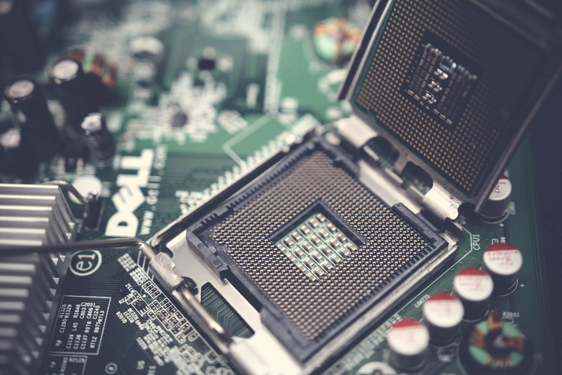
In our current electronics, most use a microchip. Microchips are highly complex circuitry used to sort and process data. Microchip fabricating is similar to the process of making printing plates for offset printing presses. Despite using some similar processes the techniques are scaled down to create an inexpensive chip capable of being used in electronics. Microchips in their early stages begin as plain sand which is almost pure silica. The sand is melted down and purified. After purification, the melted sand is turned into an ingot of pure silica. The silica is then cut into wafers and polished to a mirror finish which brings the silica smoothness to an atomic scale.
This silicon wafer becomes the platform upon which the microchips will be etched. Next, the silicon wafer has a thin layer of Silicon Dioxide (SiO2) fused to the top which is called Doping. Other chemical combinations can be added to change the properties of certain sections of the chip. On top of this layer of Silicon Dioxide, a chemical called Photoresist is added. You may recall Photoresist is the same chemical used in screen printing. Instead of being put on a silk screen, where the chemical would be burnt away, leaving blank areas of the screen, the Photoresist will remove unwanted Silicon Dioxide from the microchips. So with microchips, another step must be added because the chips need to be tiny enough for practical use. During the burning process of the chip, a black and white film is run between a UV light and a lens which miniaturizes whatever was on the film. Anywhere there is light showing through the film the Photoresist will cure. Any uncured areas will be washed away later in an acid wash. The acid wash removes the Photoresist that has not been burned and washes off the Silicon Dioxide leaving behind an etched pattern on the board. Other processes can fuse conductive metal, such as gold, onto the Silicon Dioxide pathways that have been etched as well. Additional layers of overlapping circuitry can also be added if desired.
Once the chips have been created they are tested to make sure they are fully working and they are sorted out from the non-functioning chips. The silicon wafer is then carefully cut so the chips can be separated and put into electronic items.